

IGBT structure
It includes a three-terminal device: gate G, collector C and emitter E (as shown in the attached figure).
The figure shows a-N-channel VDMOSFET combined with GTR - N-channel IGBT.
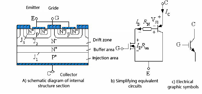
The IGBT has an additional layer of P+ injection area than the VDMOSFET and has a strong through-current capability.
The simplified equivalent circuit shows that the IGBT is a Darlington structure consisting of a GTR and MOSFET, a PNP transistor with a thick base region driven by the MOSFET.
RN is the modulation resistance within the base region of the transistor.
Characteristics of GTR - Bipolar type, current driven, with conductance modulation effect, very high through-current capability, low switching speed, high driving power required. Current control element.
Advantages of MOSFET - unipolar type, voltage driven, fast switching speed, high input impedance, good thermal stability, voltage control element.
IGBT Features
The gate is voltage-driven, the driving circuit is simple, and the driving power required is small.
High operating frequency, small switching loss, only 1/10 of GTR when the voltage is above 1000V.
High withstand voltage, high current-carrying density, high input impedance, small through-state voltage drop, good thermal stability, no "once-through" problem.
Simple driving circuit, large safe working area, strong current handling capability, no buffer circuit.
It is possible to achieve high current control with small voltage.
Stay connected
Be the first to know about our new product launches, latest blog posts and more.
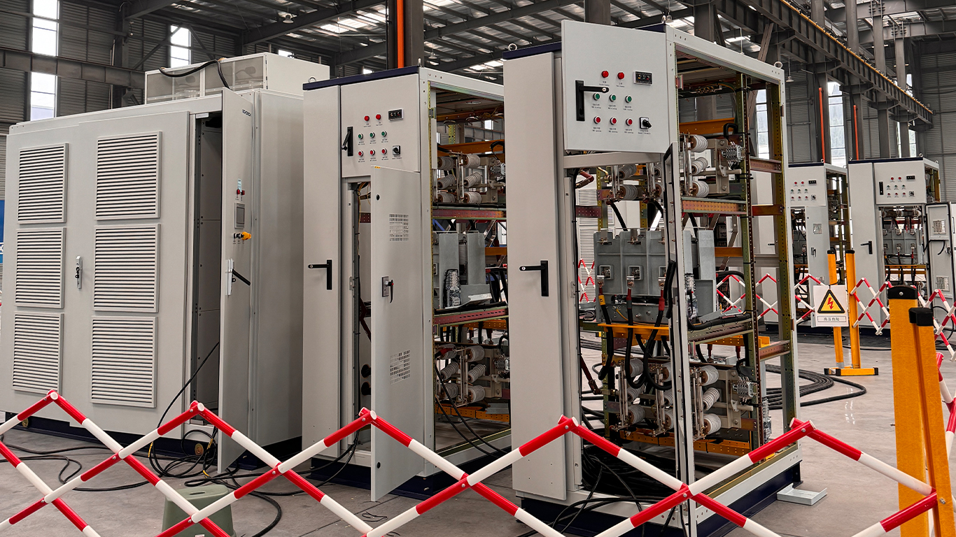
The production base of Schorch Electric Co., Ltd. is located in Suining City, Sichuan Province. It adopts the advanced technologies and manufacturing techniques of Europe. The production technologies are advanced, stable and reliable.
Any question or request?
Click below, we’ll be happy to assist. Contact us